Hobby · Aug 2026
Indoor air-quality monitor PCB
A battery-powered Home Assistant node I designed in KiCad, had assembled at JLCPCB, and then had to debug until it actually ran off an 18650. The interesting part is not the BOM. It is the datasheets I trusted, the one diode I added “to be safe,” and what the current draw looked like once the firmware was honest.
The weather-station project had already proved the software path: ESP32, ESPHome, Home Assistant. That board was a pile of AliExpress breakouts. Fine for a prototype, terrible as a product you leave in a bedroom. This time the constraint was the opposite: one small PCB, USB-C charge, a single 18650, weeks of life, and sensors that report temperature, humidity and air quality without me opening a laptop.
Hypothesis and constraints
Hypothesis: if I copy a known-good lithium charge/protect circuit, keep the ESP32 in deep sleep, and pick sensors with a documented low-power mode, an 18650 should last on the order of weeks, not days.
Constraints I wrote down before drawing a net:
- Must live on the same Wi-Fi / Home Assistant instance as the rest of the apartment.
- USB-C for charge and programming — no extra UART dongle if I can avoid it.
- Single-cell 18650, with charge and protection on-board. No “trust the cell.”
- Antenna keep-out as Espressif draws it, not as it looks pretty in 3D.
- JLCPCB assembly, so every part needs an LCSC number and a footprint they can pick.
- Small enough for a printed case, with mounting holes decided before fab, not after.
Datasheets, not forums
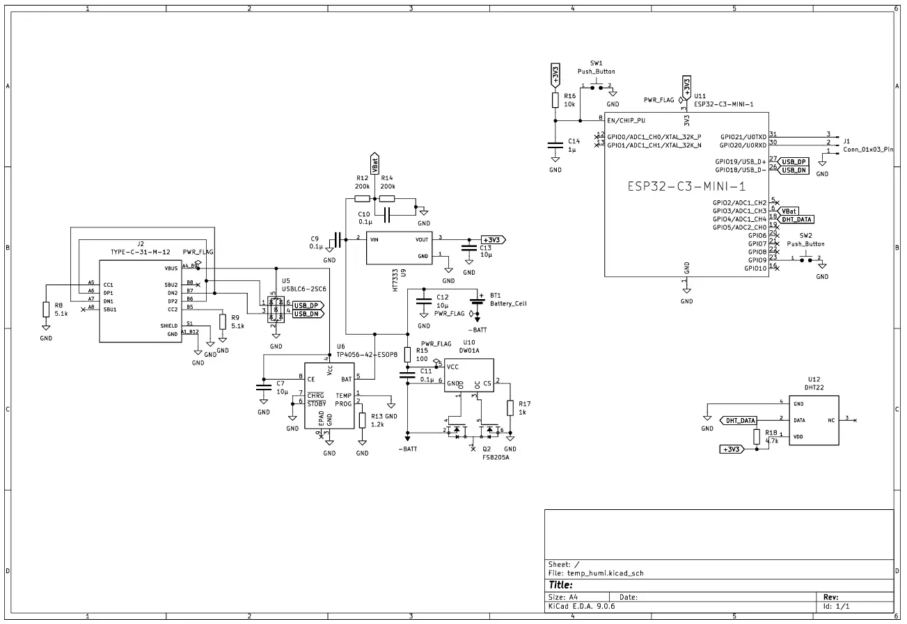
I started from the parts, not from a reference design blog.
The MCU is an ESP32-C3-MINI-1-N4X. The module datasheet is explicit about the antenna: a copper-free keep-out, module on the board edge, no ground pour under the meander. The C3 also has native USB Serial/JTAG on IO18/IO19, which is why USB-C could be both the charger and the programming port. CC1/CC2 each get 5.1 kΩ to ground so a USB-C host actually sources 5 V. D+/D− go through a USBLC6-2SC6 ESD clamp.
Charge and protect is the usual three-chip set I had already reverse-engineered on a TP4056 module: TP4056 (constant-current / constant-voltage to 4.2 V), DW01A (over-charge / over-discharge / over-current), FS8205A dual N-MOSFET on the cell negative. The DW01 datasheet is short and unforgiving: VCC must see the cell positive through ~100 Ω. If it does not, the protection FETs stay off and the board is dead on battery.
First pass of the schematic used a DHT22 and an HT7333 3.3 V LDO — enough to learn KiCad and the power path. That layout is below. The board I actually sent to fab is the next revision: SHT40 (I2C 0x44) instead of the DHT22, and a ScioSense ENS160 (I2C 0x52) for AQI / eCO2 / TVOC. The ENS160 datasheet is why the board became four layers. The analog core wants 1.8 V, the digital IO wants 3.3 V, and both rails have to be up together. I used an AP2112K-3.3 for the MCU/IO rail and an NCP163ASN180T1G for the analog rail, with the usual 100 nF + bulk next to each pin as the datasheets ask.
Layout
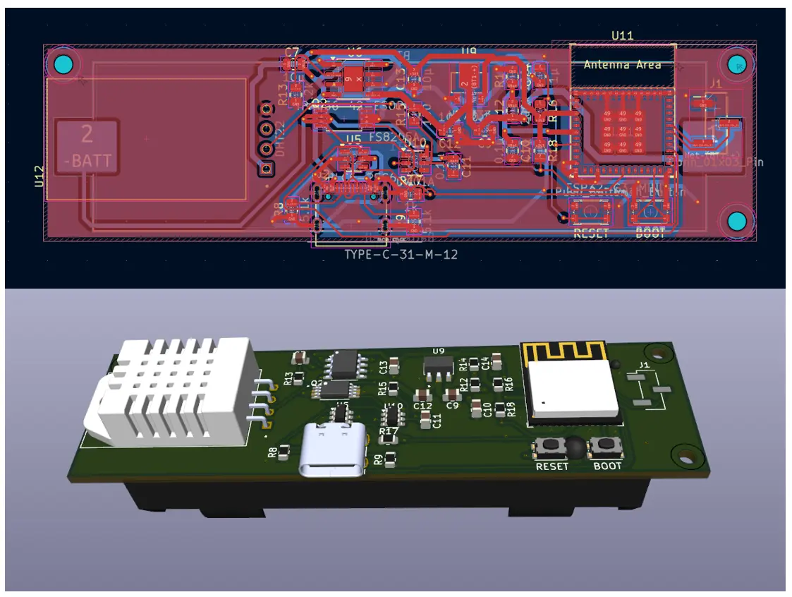
The first board was two layers, 90.5 × 25 mm, 18650 holder on the back, SMD on the front. Antenna keep-out is the hashed box on the top-right of the editor view. The assembled air-quality version is four layers (F.Cu / In1.Cu / In2.Cu / B.Cu), 95.0 × 28.9 mm, three M2 holes. Inner layers carry ground and the 3.3 V / 1.8 V pours so the ENS160 analog is not sitting on a two-layer soup of USB and RF.
JLCPCB got Gerbers, a BOM with LCSC numbers, and a CPL with rotations checked against their assembly preview. 32 unique assembly lines. The 18650 holder and a fallback UART header are DNP — hand-soldered after the panel comes back.
The SS24
This is the failure I would talk about in an interview.
Cheap TP4056 modules wire BAT straight to the cell. I decided that was sloppy. I dropped an SS24 Schottky (D8) between the TP4056 BAT pin and +BATT, the idea being reverse-current protection if USB and the cell ever fought. On paper it looks adult. In the DW01 datasheet it is a bug.
R15 (100 Ω) still went to the charger BAT pin — the anode side of D8 — not to the cell. With USB unplugged, DW01 VCC is sitting behind a diode that is not conducting. Protection FETs open. Measured on the bench:
- +BATT to GND: ~1 V, flickering.
- −BATT to GND: ~3 V (the FET is off, so “ground” on the cell negative is not board ground).
- 3.3 V and 1.8 V LEDs blinking, not solid.
- Both TP4056 LEDs (CHRG and STDBY) on at once while “charging,” then charge stopping around 3.88 V — the diode drop plus a DW01 that never saw a real cell voltage.
Continuity on a bare PCB confirmed it: BT1+ to DW01 pin 5 is open. U6.BAT to R15 to DW01 pin 5 beeps. I then opened a TP4056 breakout I trust. Same DW01 / FS8205 wiring as mine — and no diode in that line. The SS24 was my addition. I desoldered D8 and shorted the pads. The board runs off the cell. Charge termination also stopped being early, because the charger and the protection IC finally agree on what “battery voltage” is.
Lesson I will not forget: a protection IC’s VCC is not a convenient place to get creative. If the reference module omits a part, find out why before “improving” it.
Bring-up, then the firmware lies
USB-C enumerates as Espressif USB-JTAG (VID 303A). I2C scan finds 0x44 (SHT40) and 0x52 (ENS160). Firmware version 5.4.6. Home Assistant still showed ENS160 as unknown for more than an hour.
The datasheet again: after first power-up the ENS160 stays in Initial Start-Up (validity = 2) for up to ~1 h, and NEWDAT is still set. Stock ESPHome treats that flag as “do not publish.” The sensor was working. The driver was dropping the samples. I overrode the component locally so Preliminary readings go to HA, and I skip OPMODE_RESET on wake — a soft reset restarts that one-hour timer every deep sleep, which is the last thing you want on a battery node.
Temperature was also “wrong”: 32 °C in a 27 °C room. That is PCB self-heat (ESP + LDOs + ENS160), not a bad SHT40. I keep the raw board temperature for ENS160 compensation and expose a room value with a tunable offset. Humidity is the same idea, integer, with its own offset.
The current that would not sleep
A “full” 18650 at 19:40 was at 90 % by 01:00 and 86 % by 11:00. That looks like two days of life. Most of the first drop was surface charge (4.23 V → 4.10 V), not capacity. After the voltage settled, the real drain was still ugly: on the order of 7–9 mA average on a new cell. Deep-sleeping the ESP every 20 minutes barely moved it.
The ENS160 datasheet is blunt. Standard mode is ~15–29 mA. Idle is ~15 µA. I had left it in Standard 24/7 because the ESP was asleep and I assumed “the sensor is small.” It was the largest load on the board. Power LEDs (470 Ω and 220 Ω) are the next ones — they do not have a sleep pin.
Software fix: before ESP deep sleep, write OPMODE 0x01 (Idle) over I2C. On wake, if the chip is already Idle or Standard, go to Standard without reset. Sleep 30 min, wake long enough for the gas heater to leave the 400 ppm / AQI-1 floor (that floor is what you get if you only stay up 25–60 s). Duty cycle is now the ESP and the ENS160 together, not the ESP alone.
One more firmware trap, because deep sleep is a reset: ESP-IDF marks a new OTA image valid only after safe-mode’s boot_is_good_after (default 60 s). A 25 s run looks like a crashed boot. The bootloader silently restored the previous firmware after the first nap. I now confirm the image as soon as Home Assistant connects.
Battery percentage is a piecewise map of resting voltage, not 0–4.2 V scaled to 0–100 %. 4.10 V is ~97 %, not 90 %. The 4.23 → 4.10 V sag after unplug is surface charge. Using % without saying that is how you convince yourself a new cell is dying overnight.
Where it stands
Two boards are in the apartment, named separately, encrypted API, OTA, deep sleep. They report into Home Assistant. The SS24 is a solder blob. The ENS160 idles while the ESP sleeps. The case is a DXF/STEP export of the board outline and holes — the plastic is the next mechanical pass, not this one.
I would still unsolder the always-on power LEDs if I wanted calendar life instead of week life. Hardware current you forget to spec will beat any firmware duty cycle.
Learnings
Read the protection IC datasheet as carefully as the MCU one. A Schottky in a battery path is not free — it changes who sees the cell. Dual-rail sensors (1.8 V analog / 3.3 V IO) are why you pay for four layers. Drivers lie about “unknown” when the part is still warming up. Deep sleep and OTA rollback interact. Voltage is not state of charge until the surface charge is gone. And the current you do not put to sleep — gas sensor in Standard, LEDs — is the current you live with.